|
IRG-I: Synthesis and Transport in II-IV-V Chalcopyrites for Photovoltaics
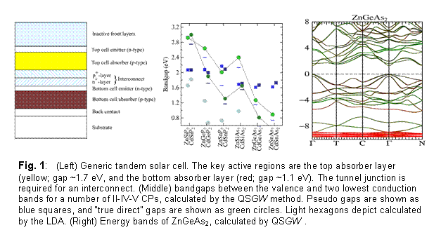
We propose to synthesize and investigate structure-property relationships of a little-studied class of thin films, the II-IV-V chalcopyrite (CP) semiconductors, with the final aim of designing and implementing an efficient, low-cost tandem thin film photovoltaic (PV) cell.
This family was deliberately selected because it meets several key criteria:
(1) A wide range of bandgaps is possible, with much flexibility in controlling other key properties such as mobility, reverse saturation current J0, and lattice-matching.
(2) The constituents are abundant, obviating a critical limiting factor (which is only beginning to be appreciated) when production reaches broad scale.
(3) High efficiencies should be possible. The II-IV-V CPs are cousins of III-V zincblende compounds. All efficient PV devices made to date derive from four-fold inorganic semiconductors.
A successful realization of an efficient stable, low-cost thin-film cell constructed out of inexpensive and abundant materials would be transformative to the PV industry and to society as a whole. The path we are proposing has a realistic chance of succeeding in that aim. We also propose a seed project that will develop and investigate organic semiconductors enhanced with metal complexes. While this latter path has the potential to be more revolutionary, the barriers to generating devices efficient and stable enough to be viable are very challenging.
Materials Selection by Design
From the beginning, our materials selection and synthesis will be guided by and closely coupled to theoretical predictions†, developing and applying the most advanced electronic structure and transport methods available. ZnSnP2 and ZnGeAs2, with gaps 1.66 and 1.15 eV. These compounds are rather similar to GaAs and also nearly lattice-match each other. Though they will be the material we will initially study, there are other attractive possibilities: ZnSi1-xGexAs2, with x~0.45, and Cd1-xZnxSi2, with x~0.3, are predicted to have a gap ~1.7 eV. Yet another alternative is the simple and well understood III-V alloy, Al1-xGaxAs.

Film Synthesis and Characterization
Knowledge of phase diagrams and kinetic barrier energies can be used to guide experiments in order to realize high quality film growth. It is even possible at times to grow metastable material (GaN and AlN are example). Initially, we will synthesize, by MBE, films of as high quality as possible. We will use available published data along with our own measurements of key thermodynamic and kinetic parameters, and ab initio total-energy calculations when needed, to design new films. This will be essential for determining thin-film growth methods and conditions that can produce single-crystal materials. Our investigations will begin with MBE films of ZnSnP2 and ZnGeAs2. In later stages we will progress into less expensive methods of synthesis, such as sputtering and MOCVD. We have extensive experience with pulsed laser deposition (PLD) —not a large-volume synthesis method but are suited to research investigations.
With good quality MBE films we will study fundamental materials properties: structural quality and defect populations, optical response, scattering mechanisms through transport measurements, recombination rates, and a possible order-disorder transition in the arrangement of II and IV atoms on the cation lattice and we will attempt to develop the ability to dope n and p type with appropriate dopants. The knowledge base for these new thin films will be developed in this project. For this we will use ASU’s excellent facilities, which include Rutherford Backscattering Spectroscopy (RBS), scanning Auger, X-ray photoelectron spectroscopy (XPS), diffraction spectroscopy (XRD), and high resolution electron microscopy. They give important information about the structure and composition of primary and secondary phases, the orientation of the films, evidence of grain size and strain, and location of native and impurity point defects.
Once high quality materials have been made, we will focus significant effort on synthesis of a series tandem thin film cell. The details of its construction will depend on our ability to dope top and bottom layers both n and p type. If this is possible, the p/n junction in a given layer can be a homojunction. This is the simplest, and likeliest to minimize recombination losses. If not, traditionally the top layer is a wide-gap n-type material such as CdS, and the absorber layer is doped p type. In the present case, there is a wide flexibility in the materials choice: we may be able to form a heterojunction of all II-IV-V CPs, which should enable synthesis of a high-quality interface. To isolate the two active regions, a low resistance n+ /p+tunnel junction must be interposed between them. Once again, the strategy we adopt will depend on our success in finding II-IV-V CPs that can doped both n and p type.
|